
Gold-plated circuit boards
Gold plated circuit boards
For applications with increased corrosion protection requirements, gold-plated circuit boards are often used. These high-quality printed circuit boards are already convincing by their appearance.
However, this consideration is superficial in the literal sense.
For price reasons, the gold layer is very thin and therefore not pore-tight.
Lasting and increased corrosion protection is not possible in this way.
To prevent the gold from migrating in the copper over time, a 3 to 4 µm thick nickel layer is applied as a diffusion barrier before the gold plating.
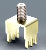
Gold-plated circuit boards should only be used if gold-plated contact surfaces must be present on the circuit board, e.g. for reeds for direct connectors, edge connectors. But even then selective gold-plating could be considered.
Together with press-fit contacts, gold-plated circuit boards should not be used if possible. For the press-fit technique, the expensive gold plating (gold can become very expensive again) only brings disadvantages. The problem is not the gold layer, but the nickel plating.
Nickel is much harder and more brittle than copper. Press-fit technique requires a deformation of the copper sleeve. However, this necessary deformation is usually too large for the nickel layer and it cracks. These cracks are points of attack for corrosion because three different metals are exposed in the crack.
The holding forces of the press-fit contacts are reduced, since nickel greatly reduces cold welding.
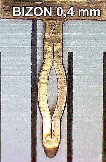
With aggressive press-fit contacts (only two contact points), the hard nickel layer easily breaks into tiny pieces during press-fitting, which wedge between the copper sleeve and the contact. The result is a violent friction welding during the press-fit process. This can be recognised by a significant increase in the press-in force. This welding can be so violent that pieces of the copper sleeve are torn out and the press-fit connection is destroyed.
The difference whether this happens or not is usually due to a slightly smaller hole diameter, which is not objectionable according to the standard. Hole diameters that are 0.02 to 0.03 mm smaller within the hole tolerance are sufficient to cause total damage.
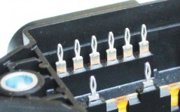
If a total gold plating of the PCB cannot be avoided, very elastic press-fit contacts with four contact points should be used. Four contact points reduce the necessary deformation of the copper sleeve by 50% compared to contacts with two contact points. A damaging friction welding can thus be avoided.
If a profound knowledge of press-fit technology is not available, early consultation avoids problems, failures and complaints that may occur later.